fig 3 The structure of external font C1
In this description, the starting point of offset address(indicate in [ ], hexadecimal) is the top of 1st block. Therefore, the data from [0000] to [0009] are 1st block of cloning data, from [000A] to [0011] are 2nd block and [0012] and later are 3rd block.
An item which marked with "?" is incorrect.
The infomation which is written in green area is offered from Mr Jim Mitchell (The author of VX7 Commander). Special thanks are due to Jim for supporting my site.
Probably, 1st and 2nd block of cloning data([0000] - [0009] and [000A] - [0011]) included the model (or version) ID of VX-7(R).
I tried to put the cloning data which got from VX-7 on VX-7R, but VX-7R indicated "CLONE ERROR" before the finish of cloning data transmitting. VX-7(R) may compare ID in the beginning of cloning and if it is different, VX-7(R) may indicate "CLONE ERROR" and aborts cloning.
This results means that the direct cloning between VX-7 and VX-7R is impossible.The possibility of the direct cloning between different version of VX-7R is unknown.
NOTE:My VX-7R is Southeast-Asian version probably. Not US nor Euro version.
| [0006] : Current Hardware
Setting [0007] : CPU Version Byte 1?? 00:Jap 01:US 03:Euro [0008] : CPU Version Byte 2?? 00:Jap 01:US 02:Euro [000A] : "Virtual Jumper Byte" (Changes "Current Hardware Setting" [0006]) E0H:US Unmodified F0H:US MARS/CAP Modification E8H:US Freeband Modification F8H:Japanese Default [000B] : Unknown?? 01 in US VX7 and 00 in Japanese VX7 [000C] : Wide/Ham RX 01 or 02:Wide RX 00:Ham only RX [000D] : Wide/Ham TX (Must also have proper "Virtual Jumper" setting) 01H:Wide TX 00:Ham Only TX |
Mr Jim Mitchell reported that if [0006], [0007], [0008] does not match radio, causes "CLONE ERROR".
| [05BA] and [063A] : FFH
all memory groups are NOT used. 00H Some memory groups are used [05BB] and [063B] : Number of memory group - 1 |
[05BB] and [063B] are the number of memory group which used
lastly - 1.
For example, if memory group 2 is used(recalled) lastly, 01H is
stored in [05BB] and [063B].
| [0611] : The sum total
of [0592] to [0610] [0691] : The sum total of [0612] to [0690] |
From [0012] to [0091], from [0092] to [0111],....from [0612] to [0691] (each 128 byte) have same format.
The data from [0592] to [0611] and from [0612] to [0691] are
same, and may include current status of VX-7.
Others (from [0012] to [0091], from [0092] to [0111],...) may
be related to "Hyper Memory".
I think that we will get many infomation about current status of VX-7 in this area but it will be very difficult.
| [0692] : the squelch level
for N-FM [0694] : the squelch level for W-FM |
|
[0695] 1XXXXXXX:VFO mode Band 0XXXXXXX:VFO mode All X1XXXXXX:CD ID ON X0XXXXXX:CD ID OFF XX1XXXXX:Scan lamp ON XX0XXXXX:Scan lamp OFF XXX1XXXX:Spec analyzer 2 ON XXX1XXXX:Spec analyzer 2 OFF XXXX1XXX:ARS ON XXXX0XXX:ARS OFF XXXXX1XX:Key beep ON XXXXX0XX:Key beep OFF XXXXXX1X:Split tone ON XXXXXX0X:Split tone OFF XXXXXXX1:DTMF Dialer ON XXXXXXX0:DTMF Dialer OFF |
|
[0696] 1XXXXXXX:BUSY LED ON 0XXXXXXX:BUSY LED OFF X1XXXXXX:Language-Jap X0XXXXXX:Language-Eng XX1XXXXX:Band link ON XX0XXXXX:Band link OFF XXX1XXXX:BCLO ON XXX0XXXX:BCLO OFF XXXX1XXX:Edge beep ON XXXX0XXX:Edge beep OFF XXXXX1XX:Hyper Write Enabled XXXXX0XX:Hyper Write Disabled XXXXXX1X:Mute Set ON XXXXXX0X:Mute Set OFF XXXXXXX1:TX Save ON XXXXXXX0:TX Save OFF |
|
[0697] XX1XXXX:Smart Search continuous XX0XXXX:Smart Search 1sec XXX1XXX:Spec-Analyzer 1 continuous XXX0XXX:Spec-Analyzer 1 1sec XXXX0XXX:15sec XXXX1XXX:25sec XXXXXX1X:Home/Rev key-Rev XXXXXX0X:Home/Rev key-Home XXXXXXX1:Moni/T-Call key-T-Call XXXXXXX0:Moni/T-Call key-Moni |
|
[0698] XXX1XXXX:Altitude unit-M XXX0XXXX:Altitude Unit-ft XXXX1XXX:Temp unit-Fahrenheit XXXX0XXX:Temp unit-Centigrade XXXXX1XX:DCS complement Enabled XXXXX0XX:DCS complement Disabled XXXXXXX1:Memory write mode-Next XXXXXXX0:Memory write mode-Lower |
|
[0699] 1XXXXXXX:Mon-F Change-Mon 0XXXXXXX:Mon-F Change-Func X1XXXXXX:Icon On Splash Screen??? X0XXXXXX:No Icon on Splash Screen??? XX1XXXXX:WX alert ON XX0XXXXX:WX alert OFF XXX1XXXX:Mic monitor ON XXX0XXXX:Mic monitor OFF XXXXX1XX:ATT ON XXXXX0XX:ATT OFF XXXXXX1X:OFF timer ON XXXXXX0X:OFF timer OFF XXXXXXX1:ON timer ON XXXXXXX0:ON timer OFF |
| [069A] : 0:OFF 1:High 2:Low |
| [069B] : 0:0.5sec 1:1sec 2:2sec |
| [069C] : 0:BEEP+Strobe 1:BEEP 2:Strobe1 3:Strobe2 4:Strobe3 5:Strobe4 6:Strobe5 7:BEAM |
| [069D] : 09H:1 0CH:2 0FH:3 12H:4 15H:5 18H:6 1BH:7 1EH:8 21H:9 24H:10 |
| [069F] : XXXXXX00:Key XXXXXX01:Continue XXXXXX10:OFF |
| [06A0] : ON timer(Hours) [06A1] : ON timer(Minutes) |
| [06A2] : OFF timer(Hours) [06A3] : OFF timer(Minutes) |
| [06A4] : 0:ALL 1:RX 2:TX |
| [06A5] : 0:hPa 1;mBar 2:mmHg 3:inch |
| [06A6] - [06A7] : 0-65535 |
| [06A8] - [06A9] : 0-65535 |
| [06AA] : 0:3sec 1:5sec 2:10sec 3:Busy 4:Hold |
| [06AC] : 0:OFF 1:200msec 2:300msec 3:500msec 4:1sec 5:2sec |
| [06AD] : 0:5MHz 1:10MHz 2:50MHz 3:100MHz |
| [06B0] - [06BF] : Callsign for CD ID |
The charactor code of the callsign is as same as charactor
set 0 and stored in the odd offset of this area. The even offset
is 00H.
If user's callsign for CW ID is not stored, all of this area are
filled with FFH.
| [06E0] : 0:OFF 1:30min 2:1hour 3:3hours 4:5hours 5:8hours |
| [06E1] : 0:OFF 1:1min 2:2.5min 3:5min 4:10min |
| [06E2] : 0:OFF 1:1 2:3 3:5 4:8 5:Continue |
| [06E3] : 0:None 1:Temp 2:Baro 3:Alti 4:Temp+Baro 5:Temp+Alti 6 :All 7:WX |
| [06E4] : Meter Number - 1 |
| [0707] : 0:OFF 1:ON |
| [0708] - [070A] : LED
color palette 1 [070B] - [070D] : LED color palette 2 [070E] - [0710] : LED color palette 3 [0711] - [0714] : LED color palette 4 [0715] - [0718] : LED color palette 5 [0719] - [071B] : LED color palette 6 [071C] - [071E] : LED color palette 7 [071F] - [0721] : LED color palette 8 [0722] - [0724] : LED color palette 9 [0725] - [0727] : LED color palette 10 |
Each palette is consist of 3 byte. The 1st is degree of RED, 2nd is GREEN and 3ed is BLUE.
| [0728] : Main BUSY [0729] : Sub BUSY [072A] : DUAL BUSY [072B] : Main TX [072C] : Sub TX [072D] : CHG Complete |
The Value is LED coloe palette number - 1 or "10".
Mr Jim Mitchell expects that "10" means LED OFF.
| [0730] : 0:Key 1:Dial 2:Key+Dial 3:PTT 4:Key+PTT 5:Dial+PTT 6:ALL |
|
[0742] : FFH Memory assigned to memory group 1 is NOT
exist. 00H Memory assigned to memory group 1 is exist. [0744] : FFH Memory assigned to memory group 2 is NOT
exist. 00H Memory assigned to memory group 2 is exist. (Abbreviation) [0752] : FFH Memory assigned to memory group 9 is NOT
exist. 00H Memory assigned to memory group 9 is exist. |
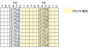
| [0754] - [0769] : External
font1(C1) [076A] - [077F] : External font2(C2) [0780] - [0795] : External font3(C3) [0796] - [07AB] : External font4(C4) [07AC] - [07C1] : External font5(C5) |
VX-7 has 5 font memory which may be created by the user. External font of VX-7 is consist of 10dot(width) * 11dot(height).
For example, the data of external font C1 is following.
It is possible for VX-7 to handle about 200 items of kanji, but Japanese people are using about 1000 - 2000 items of kanji in daily life. Therefore external font of VX-7 is important for Japanese. But editing the font using the keyboard of VX-7 is very troublesome.
| [07C2] - [07D1] : DTMF
autodialer 1 [07D2] - [07E1] : DTMF autodialer 2 [07E2] - [07F1] : DTMF autodialer 3 [07F2] - [0801] : DTMF autodialer 4 [0802] - [0811] : DTMF autodialer 5 [0812] - [0821] : DTMF autodialer 6 [0822] - [0831] : DTMF autodialer 7 [0832] - [0841] : DTMF autodialer 8 [0842] - [0851] : DTMF autodialer 9 |
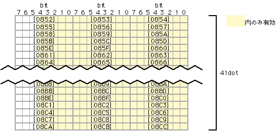
| [0852] - [08CC] : Icon1(I1) [08CE] - [0948] : Icon2(I2) [094A] - [09C4] : Icon3(I3) |
VX-7 has 3 icon memory which may be created by the user. External icon of VX-7 is consist of 21dot(width) * 41dot(height).
For example, the data of external icon I1 is following. The bit in yellow area is effective. [08CD] is meaningless.
The infomation of home memory may be stored in this area. The format is as same as regular memory.
In case of VX-7 and VX-7R(expect for US version), 220MHz BAND is not exist. Is [0CE6] - [0CFB] for 220MHz BAND? It is unknown, because I do not have US version on VX-7R.
|
[0C62] - [0C77] : BC BAND *Not used except for US version. |
This is an estimate, too. The format may be as same as regular memory. [0E72] - [0E87] of my VX-7 is filled with FFH. This may be the wreckage of 220MHz SUB VFO??
|
[0D54] - [0D69] : MAIN VFO : BC BAND [0E46] - [0E5B] : SUB VFO : 50MHz BAND *Not used except for US version. |
One list includes 48 numbers of memory and One number of memory is written in 2 byte. The redundant area is filled with FFH.
0000H means memory 001, 0001H means memory 002....
|
[0EA2] - [0F01] : MG1 (Abbreviation) |
<<example>>
If memory001, 002 and 256, 257 (4 memories) are assigned to memory group 1....
[0742] : 00H
[0743] : 03H
[0EA2] : 00H
[0EA3] : 00H
{0EA4] : 00H
[0EA5] : 01H
[0EA6] : 00H
[0EA7] : FFH
[0EA8] : 01H
[0EA9] : 00H
The flag table which indicate core of memory channel is valid or not.
|
1.Regular memory [1202] bit3-0 : M001 (Abbreviation) [12E1] bit3-0 : M447 2.One-touch memory [12E3] bit3-0 : OTM1 3.PMS memory [12E8] bit3-0 : PMS_L01 (Abbreviation) [12F9] bit7-4 : PMS_U18 |
Each 4bits means following.
|
XX00:NOT valid X0XX:NOT skip memory 0XXX:NOT preferential memory |
|
1.Regular memory [1322] - [1337] : M001 (Abbreviation) [3976] - [398B] : M447 2.One-touch memory [39CE] - [39E3] : OTM1 3.PMS memory [3AAA] - [3ABF] : PMS_L01 (Abbreviation) [3DAC] - [3DC1] : PMS_U18 |
One record is composed of 22 byte(fixed field). The structure of record is following.
| offset (from the top of the record) |
contents | RMKS |
| +0 | (unknown) |
At present, unknown. However, maybe Mr Jim Mitchell expects that... |
| +1 | power level, step etc | |
| +2 | Frequency(100MHz&10MHz) | described in BCD |
| +3 | Frequency(1MHz&100KHz) | |
| +4 | Frequency(10KHz&1KHz) | |
| +5 | mode | bit7-2:Always"001100XX"?? |
| +6 | 1st charactor of memory tag | |
| +7 | 2nd charactor of memory tag | |
| +8 | 3rd charactor of memory tag | |
| +9 | 4th charactor of memory tag | |
| +10 | 5th charactor of memory tag | |
| +11 | 6th charactor of memory tag | |
| +12 | 7th charactor of memory tag | |
| +13 | 8th charactor of memory tag | |
| +14 | (unknown) | Always 00H?? |
| +15 | Frequency for transmitting(100MHz&10MHz) | described in BCD |
| +16 | Frequency for transmitting(1MHz&100KHz) | |
| +17 | Frequency for transmitting(1MHz&100KHz) | |
| +18 | Tone frequency(CTCSS) | 0 49 |
| +19 | DCS code | 0 103 |
| +20 | CTCSS/DCS | |
| +21 | charactor set of memory tag |
The frequency information of memory is described at offset +2 to +4 and +15 to +17 in BCD. In case of 12.5kHz step, the fraction of the 0.5kHz is ignored.
Offset +2 to +4 is the frequency which becomes main, in other words, is memory frequency itself.
Offset +15 to +17 is secondary frequency. In case of "-RPT" or "+RPT", this frequency means magnitude of the repeater shift. If you stored independent transmit frequencies, this means the transmit frequencies itself.
It's stored in bit 7 and 6 of offset +2.
| 00XXXXXX:L1 01XXXXXX:L2 10XXXXXX:L3 11XXXXXX:Hi |
It's stored in bit 5 and 4 of offset +2.
| XX00XXXX:Simplex XX01XXXX:-RPT XX10XXXX:+RPT XX11XXXX:Independent transmit frequencies |
It's stored in bit 3 to 0 of offset +2.
| XXXX0000:5KHz XXXX0001:10KHz XXXX0010:12.5KHz XXXX0011:15KHz XXXX0100:20KHz XXXX0101:25KHz XXXX0110:50KHz XXXX0111:100KHz XXXX1000:9KHz |
It's stored in bit 1 and 0 of offset +5.
| XXXXXX00:N-FM XXXXXX01:AM XXXXXX10:W-FM XXXXXX11:(unknown) |
It's stored in bit 1 and 0 of offset +20.
| XXXXXX00:none XXXXXX01:CTCSS encoder XXXXXX10:CTCSS encoder/decoder XXXXXX11:DCS |
It's stored in Offset +18.
|
00H : 67.0Hz (Abbreviation) 2EH : 233.6Hz |
It's stored in Offset +19.
|
00H : 023 (Abbreviation) 64H : 732 |
The each memory channel of VX-7 has the memory tag(8 charactors per memory). We can use the alpha-numeric charactors and the Japanese charactors(hira-gana, kata-kana and kanji).
VX-7 is the first HT which be able to handle hira-gana and kanji on LCD. It's a miracle advantage for radio amateurs in JA, but meaningless for hams in other many countries.
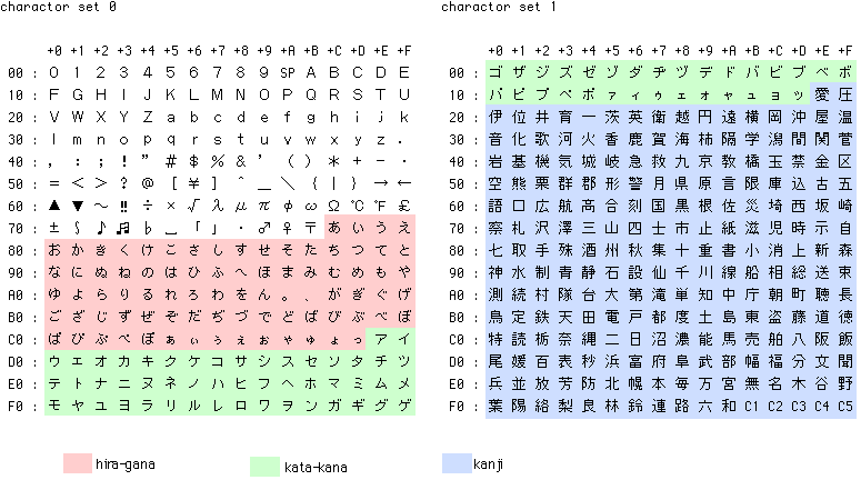
To handle the Japanese charactors, VX-7 has two charactor sets. Offset +21 indicates this.
|
XXXXXXX0 : 1st charactor of memory tag : use charactor
set 0
(Abbreviation) X0XXXXXX : 7th charactor of memory tag : use charactor
set 0
|
<<example>>
| offset +6 | offset +7 | offset +8 | offset +9 | offset +10 | offset +11 | offset +12 | offset +13 | offset +21 |
| A5H | CEH | 8CH | E4H | 27H | 2CH | 04H | 0AH |
0FH "00001111" 1st - 4th charactors are charactor set 1 |
*Japanese kanji
![]()
![]() : Osaka city
: Osaka city
![]()
![]() : fire station
: fire station
| [3F52] : The sum total of [0000] to [3F51] |
Copyright by Heian Software Engineering (C)H.S.E.
2002 Allrights reserved.
A summary in English - Created : Nov 11 2002, Last updated : Jan
28 2003